

The invention of transistors in the middle of the 20th century set the course for the electronics revolution. Transistors use a “gate” voltage to switch a semiconductor between ON and OFF states. Although a disruptive technology, owing to their reliance on an external gate, transistors are, by nature, externally powered and energy-intensive, especially with the increasing packing densities of these devices. A self-powered transistor utilizing a renewable source of energy would therefore be a potential game-changing technology.
Now a solar-powered field-effect transistor or “solaristor” has been demonstrated by the research groups of Mónica Lira-Cantú and Gustau Catalán at the Catalan Institute of Nanoscience and Nanotechnology (ICN2), Spain. Employing a ferroelectric film in the most commonly used solar-cell architecture of organic photovoltaics (bulk heterojunction), the researchers were able to switch the photocurrent of the device between ON and OFF states, utilizing absorbed photons as the gate. Importantly, the solaristor was realized as a two-electrode vertical stack architecture, significantly reducing the interconnection complexity of the conventional in-plane three-electrode transistor architecture.
Previous attempts used ferroelectric films as the absorber layer in solar cells. However, since these films are usually wide-bandgap semiconductors and, therefore, poor absorbers of the visible spectrum, photocurrents have been severely limited, leading to overall poor power-conversion efficiencies. Lira-Cantú’s group turned to the concept of an organic bulk heterojunction to absorb photons. These absorbers are solution-processed, have an optimal bandgap in the visible region, and are currently attracting intense research interest for applications in thin-film organic photovoltaics (OPVs). Utilization of these organic absorbers resulted in high photocurrents in the range of 5–10 mA cm–2.
A conventional OPV device sandwiches these absorbers between electron- and hole-extracting layers. In the present study, the researchers also included a wide-bandgap n-type ferroelectric semiconducting film at the electron-extracting electrode. The high bandgap (3.6 eV) of the ferroelectric film means that this layer is transparent to most of the solar spectrum, ensuring that maximal photon flux reaches the sandwiched organic absorber. Poling the ferroelectric by applying a DC voltage to one of the electrodes effectively tuned the band offset at the electron-collecting junction, resulting in efficient collection (ON) or blocking (OFF) of photoelectrons.
As reported in a recent issue of Advanced Functional Materials (doi:10.1002/adfm.201707099), a transparent conductive oxide made of fluorine-doped tin oxide served as the cathode while a compact thin film of Pb(ZrxTi1–x)O3 (PZT) was used as the ferroelectric layer. The organic absorber consisted of a blend of P3HT polymer (donor) and the PCBM fullerene as the acceptor. V2O5 and silver were, respectively, used as the hole transporter and the metal anode.
“This new generation phototransistor or solaristor exemplifies a transparent, compact, and light-powered optoelectronic device, which has all the right ingredients to transform the oxide electronics arena. What’s more, the device is fabricated using low-cost and scalable solution-processable techniques under ambient atmospheric conditions, paving the way for the future development of printed and flexible devices. Applications are all around us, from transparent electronics (phototransistors, photoferroelectric memories), transparent displays, and sensors, among others,” Lira-Cantú says.
Robert Hoye and Judith MacManus-Driscoll at the University of Cambridge, studying complex functional materials and nanostructures, feel that the work holds promise for the future of the photovoltaics community and market. “This report represents a new device architecture for photoswitching that could be more easily implemented with photovoltaic materials than the standard phototransistor architecture. The photovoltaics community is currently experiencing a renaissance in materials discovery, owing to the recent success of hybrid lead halide perovskites. The architecture presented by Lira-Cantú et al. could allow these new materials to flow into the photoswitching community by enabling these new materials to be more easily investigated,” Hoye and Driscoll say in an email.
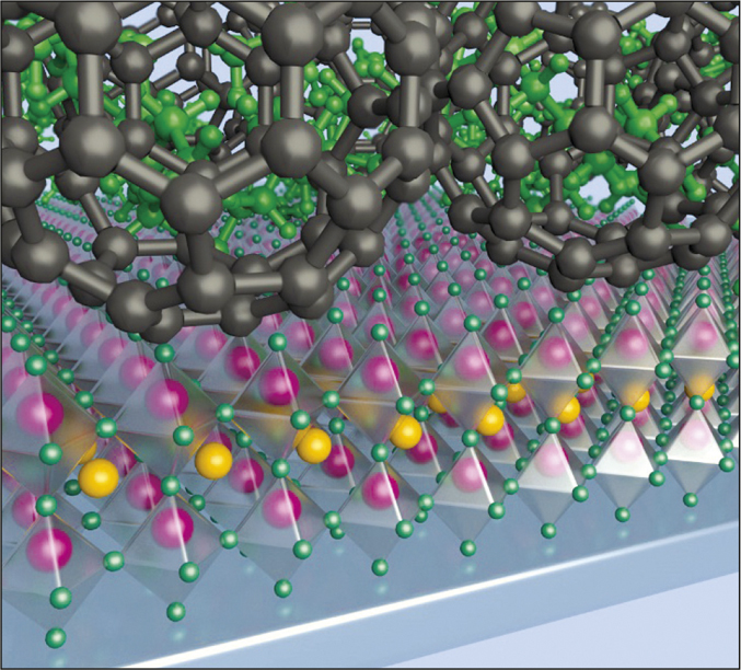
Schematic showing the active ingredients of the solaristor, organic bulk heterojunction placed atop the ferroelectric film. Credit: Mónica Lira-Cantú.
The next-generation designs of the solaristor could benefit from replacing the organic bulk heterojunction absorber, where the photocurrent is limited, with colloidal quantum dot or hybrid perovskite absorbers, which promise much higher photocurrents (22–30 mA cm–2). Importantly, since these solaristors employ solution-processed components, it might be possible in the near future to print them at industrial scales on flexible substrates in a cost-effective manner, potentially making them active components of Internet-of-Things (IoT) devices.
